
浏览量:
1014
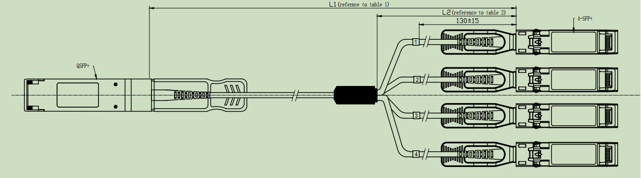
JHA-QSFP-4SFP-40G-AOC spec
零售价
0.0
元
市场价
0.0
元
浏览量:
1014
产品编号
数量
-
+
库存:
0
产品描述
产品特征
产品参数
产品描述:
产品特征:
● Support 40-4*10GBASE-SR application
● Electrical interface compliant to QSFP+ connector
(SFF-8436) and SFP+ connector (SFF-8431)
● 850nm VCSEL transmitter, PIN photo-detector receiver
● Multi rate of up to 10.3125Gbps per lane
● Operating case temperature: 0 to 70℃
● +3.3V power supply voltage
● Low power consumption
● RoHS compliant
● UL certification cables (optional)
扫二维码用手机看


7*24小时售后支持

安全技术解决方案

研究开发创新

资质认证

咨询电话:0755-81483343
产品咨询:13316858670
技术邮箱:cfc@jha-tech.com
地址:深圳市龙华区大浪街道横朗社区联建科技工业园厂房5栋3层

手机扫一扫
Copyright © 深圳市锦昊安科技有限公司 All rights reserved 粤ICP备19135367号 网站建设:中企动力 深圳